CTS Design Group

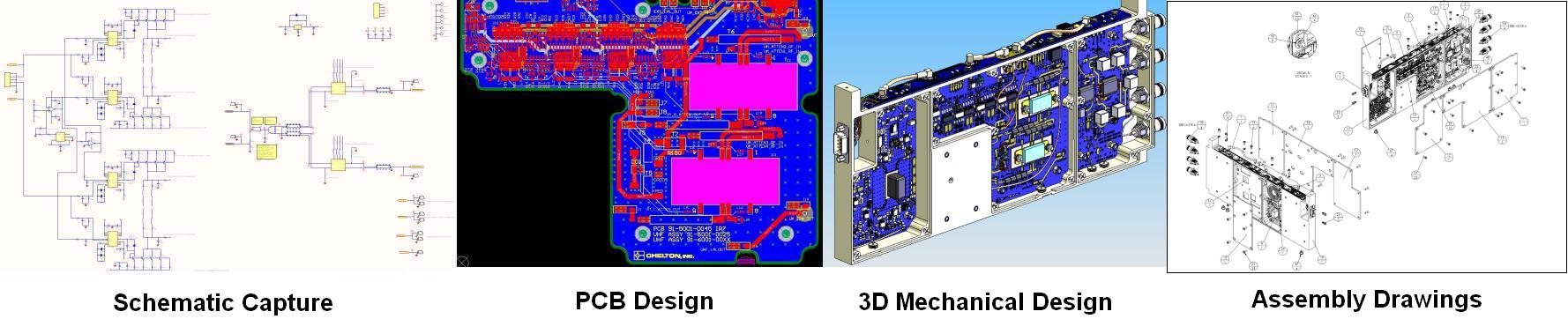
Schematic Capture
OrCAD Capture 16.6

PCB Design
Altium Designer and PADS PowerPCB 9.5
3D and 2D CAD Design and Drafting
Solidworks and AutoCAD

![]()
Welcome to CTS Design Group. We specialize in Schematic Capture, PCB Design, Schematic and PCB Foot print Libraries, Reverse Engineering, Engineering Localization and 2D and 3D CAD Design Drawings. With Fifteen years experience in the design of Printed Circuit Boards and 10 years experience in 3D Mechanical Design and Drafting, We will take care of all your technical needs. We uitilize Mentor Graphics PADS Power PCB and Altium Designer. For 2D and 3D CAD Design and drawing needs, we utilize Solidworks and AutoCAD. Please view our experience below with some of the companies worked with and feel free to contact CTS Design Group or fill out the contact form below. I am available for Part time and Contract work.
CTS Design Group
601-917-8684
pcbdesignerwork@gmail.com
Experience
Design Engineer - PCB Layout
October 2010 - Present
Toshiba International Corporation, Houston, TX

Industrial Division - Power Electronics R&D
Schematic Capture and PCB Design (OrCAD Layout 15.7 and Capture 16.3)
The Design Engineer will act as electrical designer specializing in printed circuit board designs for Toshiba’s adjustable speed drives and uninterruptible power supply product lines. The individual contributor will be responsible for drawings test plans, and design notes. Additional activities include support of manufacturing, field service, marketing and validation on a proactive basis.
Primary Functions and Responsibilities:
• Supporting new product development through through excellence in PCB layout and testing
• Managing projects and maintaining product documentation;
• Sustaining engineering for current products;
• Preparing and checking drawing and designs; and
• Performing other related duties as assigned by management.
PCB Designer (Contract)
July 2010 - September 2010
Inuve Security Products, Charlotte, NC
![]()
Privately help consumer electronics industry
Schematic Capture and PCB Design (Alitum Designer Summer 2009)
2 to 3 month contract job helping Invue Security update some of their
schematics and circuit boards for their security products. I am
currently using Alitum Designer Summer 2009 for these tasks. I am also
using the 3D feature in the software to it's full advantage as well as
helping with some light mechanical design modeling 3D parts for use in
Altium Designer. Utilizing Solid works 2010 for the mechanical design
and modeling.
PCB Designer (Contract)
June 2010 - July 2010
Aeroflex Corporation, Plainview,

Department of Defense and Aerospace Industry
Schematic Capture and PCB Design (Alitum Designer Summer 2009)
Update Schematics and PCBs from old Protel 1999 designs. I created schematic and PCB Decal libraries from existing boards to update new designs. I performed PCB updates for multi-channel “burn in boards” that were used to test the 4404 Aeroflex Hybrid IC’s. I created Gerber files and documentation packages for PCB quotes, fabrication and manufacturing.
CAD Design and Drafting (AutoCAD 2000i)
I exported DXF files from Altium Designer Gerber to create; Assembly, Drill, Fabrication and documentation drawings.
PCB Designer (Contract)
May 2010 – Present
ionDesign Incorporated, Austin,


![]()

![]()

Consumer Electronics and PCB Design Services
http://www.iondsn.com/index.html
Schematic Capture and PCB Design (Alitum Designer Summer 2009)
My job functions are schematic
capture and layout design of various consumer electronics from simple two-layer
pcbs to complex multilayer high density, high speed electronics. Other job
functions include creating schematic and PCB decal libraries and research and
development on PCB parts. I have done PCB designs for Dril-Quip and Brimtech as well as other companies through ionDesign.
PCB Design Engineer
April 2006 – November 2009
Chelton Inc. Doing Business as Cobham Antenna Systems, Cedar Rapids, IA
![]()
Department of Defense and Aerospace Industry
Schematic Capture and PCB Design (Alitum Designer 6.0+)
I performed schematic capture from preliminary block diagrams, engineering specifications, component samples and bread boarded prototypes. I researched parts needed from vendors on tolerance, power requirements and packaging specs. I Created schematic parts from datasheets and maintained them in the schematic symbol library. I extracted net-list from schematic and designed high density, mixed analog, digital and RF (30-512MHz) PCBs using Altium Designer 6.0+ software package. I Performed post processing design rule checks, post preliminary engineering checks and processed finished PCB design for Gerber creation for board vender. I transferred all design documentation to engineering server. Also performed updates to PCBs from ECN / ECO (Engineering Change Notice / Order).
CAD Design and Drafting (Solidworks 2009 and AutoCAD 2004)
I used Solidworks 2009 CAD software to generate 3D models of PCBs for mechanical test fixture, design and documentation. I generated AutoCAD/Solidworks drawings of finished PCBs containing dimensions, material, layer stack-up information for board vendor. I Created and maintained 3D Solidworks assemblies and Parts such as, metal fixtures, models of antennas, nuts and bolts, and electronic components in a CAD library. I updated antenna and SATCOM AutoCAD drawings and also maintained Microsoft Visio wiring diagrams for Rockwell Collins and Boeing customers.
Assembly, Testing and Trouble-shooting
I assembled SMT devices such as SOIC, DIP, 0601-1205 and thru-hole axial resistors and capacitors on finished PC boards for prototypes. I used bench equipment such as soldering irons, lab microscopes, SMT extractor and application tools, tested and trouble-shooted to component level PC boards using Digital volt meters, Oscilloscopes and Spectrum and Network analyzers.
Printed Circuit Board Designer
September 2000 – October 2005
Peavey Electronics Corporation, Meridian, MS
![]()
Manufacturer of Musical Equipment
PCB Design (Mentor Graphics PADS PowerPCB)
I obtained engineering specifications and design rules from electrical and mechanical engineers from marked up schematics, notes, diagrams, mechanical drawing dimensions and component samples. I obtained net-list and designed complex analog, digital and hybrid single-sided circuit boards to multi-layer ASIC & DSP technologies for pro-audio electronics such as guitar amps (Wiggy, Triple XXX), sound generators (Kosmos Pro) and mixer consuls (KB12 Keyboard amps). I adhered to strict DFM and UL (i.e. primary and secondary spacing for high voltage power supplies) guidelines. I obtained PCB quotes from vendors for competitive prototype pricing. I Performed test point placement, post processing design rule checks, post preliminary engineering checks and processed finished PCB design. I generated Gerber files, value and reference designator drawings, CAM and NC Drill files for manufacturing. I sent Gerber package to board vender for 1 to 2 day turns. I transferred all design documentation to engineering server. I also performed PCB updates from ECN / ECO (Engineering Change Notice / Order).
Electro-mechanical Assembly
I assembled prototype and “show” products for NAMM (National Association of Music Merchants) and for engineering testing. I assembled single-sided circuit boards, speaker cabinets and wired voltage supplies. I used schematics, refdes and value drawings and wiring diagrams for assembly.
Technical Writing
I documented procedures utilizing PADS software for PCB Design techniques, test point generation, post processing and Gerber file creation. I documented procedures for utilizing FAB Factory and CAM 350 for PCB post processing.